- 您现在的位置:买卖IC网 > Sheet目录1917 > DSPIC30F3013-20I/ML (Microchip Technology)IC DSPIC MCU/DSP 24K 44QFN
2011 Microchip Technology Inc.
DS39932D-page 197
PIC18F46J11 FAMILY
12.0
TIMER0 MODULE
The Timer0 module incorporates the following features:
Software selectable operation as a timer or
counter in both 8-bit or 16-bit modes
Readable and writable registers
Dedicated 8-bit, software programmable
prescaler
Selectable clock source (internal or external)
Edge select for external clock
Interrupt-on-overflow
The T0CON register (Register 12-1) controls all
aspects of the module’s operation, including the
prescale selection. It is both readable and writable.
Figure 12-1 provides a simplified block diagram of the
Timer0 module in 8-bit mode. Figure 12-2 provides a
simplified block diagram of the Timer0 module in 16-bit
mode.
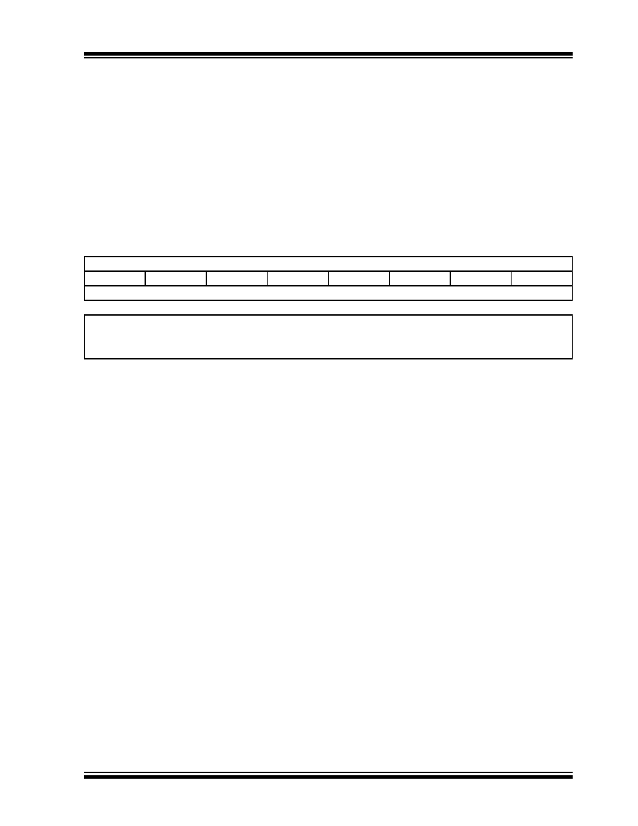
REGISTER 12-1:
T0CON: TIMER0 CONTROL REGISTER (ACCESS FD5h)
R/W-1
TMR0ON
T08BIT
T0CS
T0SE
PSA
T0PS2
T0PS1
T0PS0
bit 7
bit 0
Legend:
R = Readable bit
W = Writable bit
U = Unimplemented bit, read as ‘0’
-n = Value at POR
‘1’ = Bit is set
‘0’ = Bit is cleared
x = Bit is unknown
bit 7
TMR0ON:
Timer0 On/Off Control bit
1
= Enables Timer0
0
= Stops Timer0
bit 6
T08BIT
: Timer0 8-Bit/16-Bit Control bit
1
= Timer0 is configured as an 8-bit timer/counter
0
= Timer0 is configured as a 16-bit timer/counter
bit 5
T0CS
: Timer0 Clock Source Select bit
1
= Transition on T0CKI pin input edge
0
= Internal clock (FOSC/4)
bit 4
T0SE
: Timer0 Source Edge Select bit
1
= Increment on high-to-low transition on T0CKI pin
0
= Increment on low-to-high transition on T0CKI pin
bit 3
PSA
: Timer0 Prescaler Assignment bit
1
= Timer0 prescaler is not assigned. Timer0 clock input bypasses prescaler.
0
= Timer0 prescaler is assigned. Timer0 clock input comes from prescaler output.
bit 2-0
T0PS<2:0>
: Timer0 Prescaler Select bits
111
= 1:256 Prescale value
110
= 1:128 Prescale value
101
= 1:64 Prescale value
100
= 1:32 Prescale value
011
= 1:16 Prescale value
010
= 1:8
Prescale value
001
= 1:4
Prescale value
000
= 1:2
Prescale value
发布紧急采购,3分钟左右您将得到回复。
相关PDF资料
DSPIC30F4011-30I/ML
IC DSPIC MCU/DSP 48K 44QFN
DSPIC30F4013-30I/ML
IC DSPIC MCU/DSP 48K 44QFN
DSPIC30F5013-30I/PT
IC DSPIC MCU/DSP 66K 80TQFP
DSPIC30F5015-30I/PT
IC DSPIC MCU/DSP 66K 64TQFP
DSPIC30F6010-20E/PF
IC DSPIC MCU/DSP 144K 80TQFP
DSPIC30F6010A-30I/PF
IC DSPIC MCU/DSP 144K 80TQFP
DSPIC30F6013A-30I/PF
IC DSPIC MCU/DSP 132K 80TQFP
DSPIC30F6014-30I/PF
IC DSPIC MCU/DSP 144K 80TQFP
相关代理商/技术参数
dsPIC30F3013-20I/SO
功能描述:数字信号处理器和控制器 - DSP, DSC 28LD 20MIPS 24 KB RoHS:否 制造商:Microchip Technology 核心:dsPIC 数据总线宽度:16 bit 程序存储器大小:16 KB 数据 RAM 大小:2 KB 最大时钟频率:40 MHz 可编程输入/输出端数量:35 定时器数量:3 设备每秒兆指令数:50 MIPs 工作电源电压:3.3 V 最大工作温度:+ 85 C 封装 / 箱体:TQFP-44 安装风格:SMD/SMT
dsPIC30F3013-20I/SP
功能描述:数字信号处理器和控制器 - DSP, DSC 28LD 20MIPS 24 KB RoHS:否 制造商:Microchip Technology 核心:dsPIC 数据总线宽度:16 bit 程序存储器大小:16 KB 数据 RAM 大小:2 KB 最大时钟频率:40 MHz 可编程输入/输出端数量:35 定时器数量:3 设备每秒兆指令数:50 MIPs 工作电源电压:3.3 V 最大工作温度:+ 85 C 封装 / 箱体:TQFP-44 安装风格:SMD/SMT
DSPIC30F3013-30I/ML
功能描述:数字信号处理器和控制器 - DSP, DSC Sensor RoHS:否 制造商:Microchip Technology 核心:dsPIC 数据总线宽度:16 bit 程序存储器大小:16 KB 数据 RAM 大小:2 KB 最大时钟频率:40 MHz 可编程输入/输出端数量:35 定时器数量:3 设备每秒兆指令数:50 MIPs 工作电源电压:3.3 V 最大工作温度:+ 85 C 封装 / 箱体:TQFP-44 安装风格:SMD/SMT
DSPIC30F3013-30I/SO
功能描述:数字信号处理器和控制器 - DSP, DSC Sensor RoHS:否 制造商:Microchip Technology 核心:dsPIC 数据总线宽度:16 bit 程序存储器大小:16 KB 数据 RAM 大小:2 KB 最大时钟频率:40 MHz 可编程输入/输出端数量:35 定时器数量:3 设备每秒兆指令数:50 MIPs 工作电源电压:3.3 V 最大工作温度:+ 85 C 封装 / 箱体:TQFP-44 安装风格:SMD/SMT
DSPIC30F3013-30I/SO
制造商:Microchip Technology Inc 功能描述:IC DSC 16BIT 24KB 40MHZ 5.5V SOIC-28
DSPIC30F3013-30I/SP
功能描述:数字信号处理器和控制器 - DSP, DSC Sensor RoHS:否 制造商:Microchip Technology 核心:dsPIC 数据总线宽度:16 bit 程序存储器大小:16 KB 数据 RAM 大小:2 KB 最大时钟频率:40 MHz 可编程输入/输出端数量:35 定时器数量:3 设备每秒兆指令数:50 MIPs 工作电源电压:3.3 V 最大工作温度:+ 85 C 封装 / 箱体:TQFP-44 安装风格:SMD/SMT
DSPIC30F3013-30I/SP
制造商:Microchip Technology Inc 功能描述:16-Bit Digital Signal Controller
dsPIC30F3013T-20E/ML
功能描述:数字信号处理器和控制器 - DSP, DSC 44LD 20MIPS 24 KB RoHS:否 制造商:Microchip Technology 核心:dsPIC 数据总线宽度:16 bit 程序存储器大小:16 KB 数据 RAM 大小:2 KB 最大时钟频率:40 MHz 可编程输入/输出端数量:35 定时器数量:3 设备每秒兆指令数:50 MIPs 工作电源电压:3.3 V 最大工作温度:+ 85 C 封装 / 箱体:TQFP-44 安装风格:SMD/SMT